W. M. Keck Foundation Program for Scaling Engineering Education
“A Matter of Scale” Click Here for Videos and Presentations about Scaling Engineering
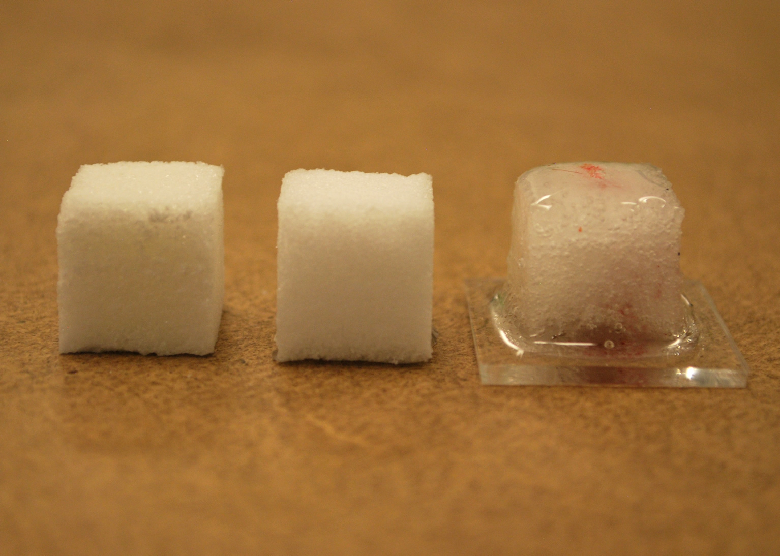
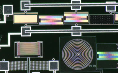
Scaling Engineering is one of our site differentiating specialties. It is becoming increasingly important to develop methods to train young people with the intuition for the way things work in the tiny world – when the surface-to-volume ratio increases to the point of rendering our familiar world implausible and non-functional at the micrometer scale and smaller. We develop curriculum support modules to convey a sense for how things work at this scale educationally, when it is so difficult and expensive to implement hands-on training.
Through funding by the W.M. Keck Foundation, we create micro learning vehicles that bridge the familiar with the new, the macro with the micro, and do this with captivating and inexpensive visual techniques for in-class demos with accompanying modular lesson plans that can be transferred to new & existing undergraduate curricula. We deploy the devices and lessons within a course dedicated to scaling engineering here at the University of Utah, followed by local distribution and national dissemination through existing peer networks.
 Please feel free to use these in classes with acknowledgement of the Keck Foundation, Sandia National Labs, the University of Utah Nanofab (PI’s I.R. Harvey, B.Baker, B. Gale, B. Raeymaekers, and TTU Professor Tim Dallas) and the specific authors and institutions responsible for the presentations and lesson plans.
Microfluidics Scaling Engineering Lesson Plans and Presentations
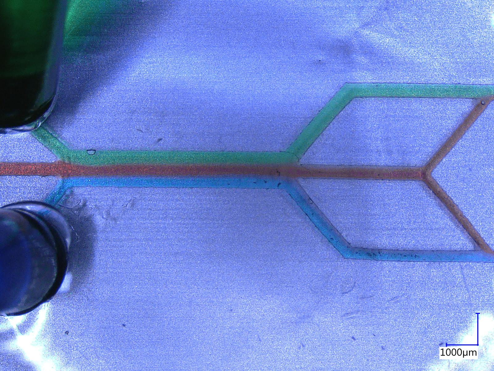
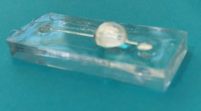
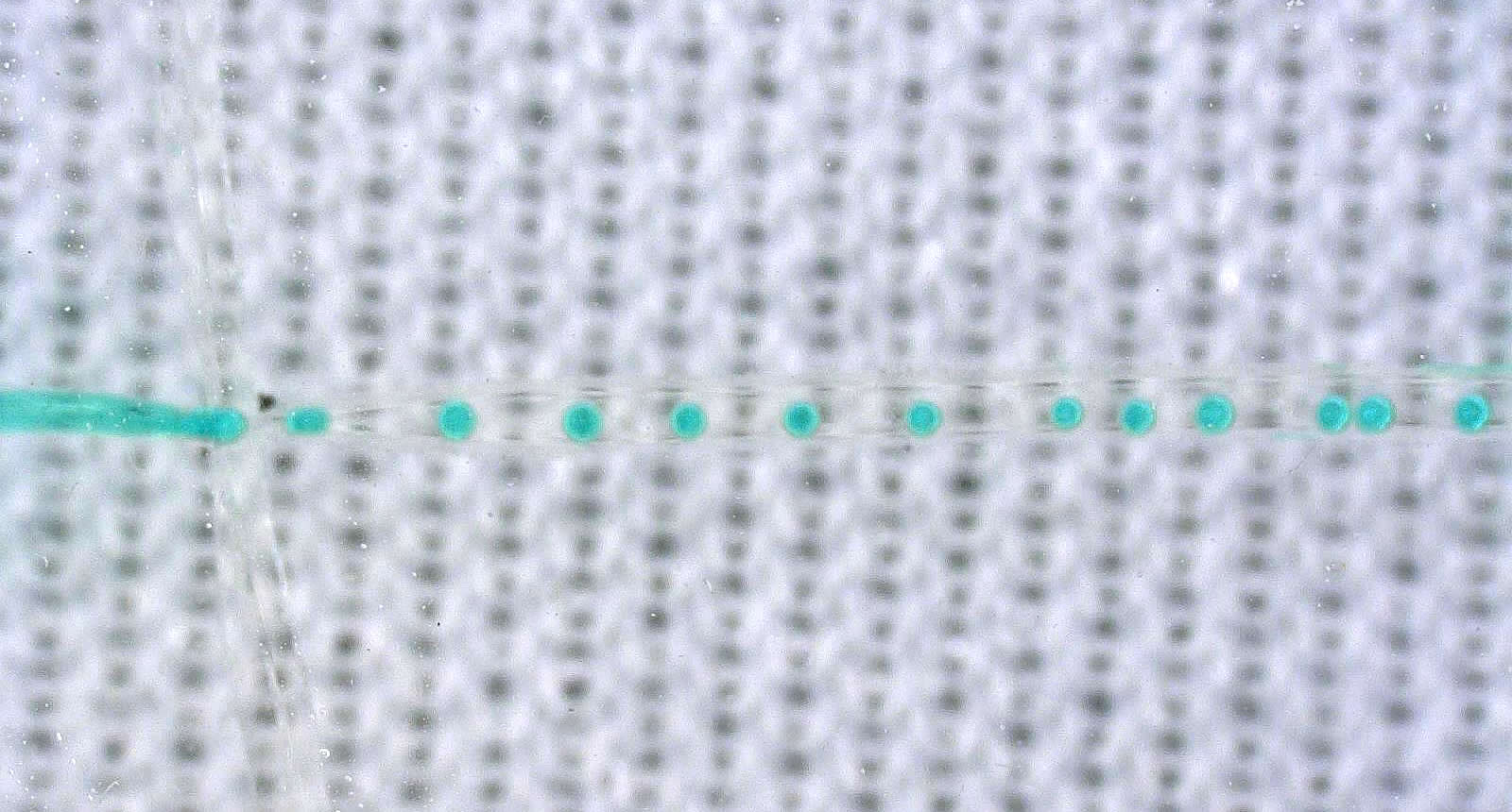
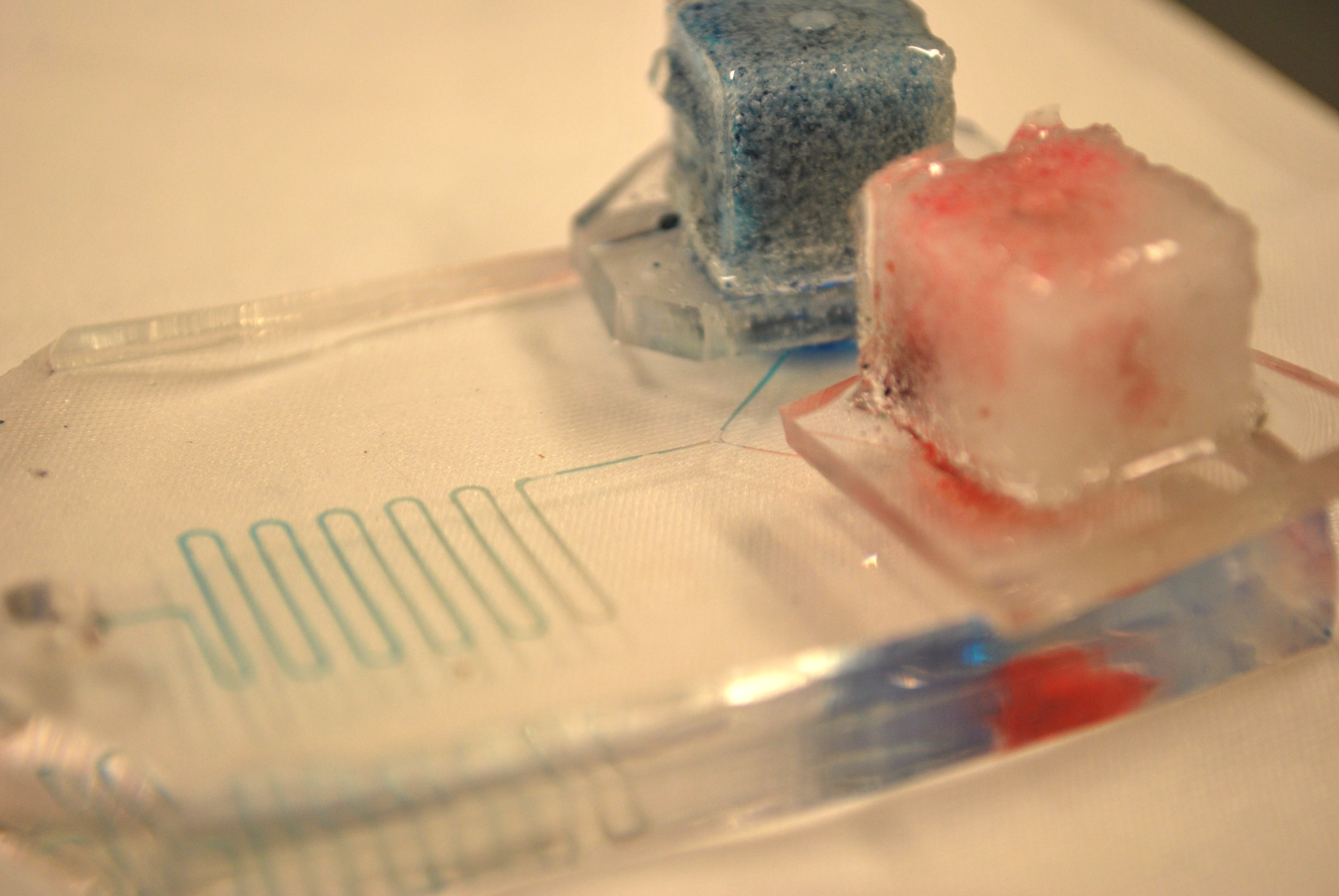
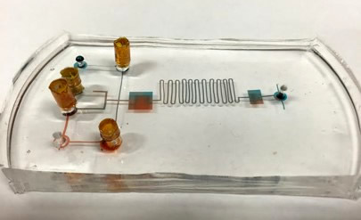
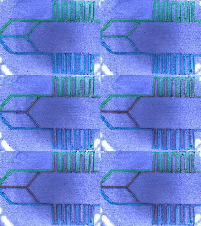
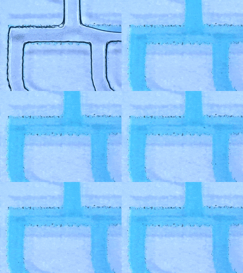
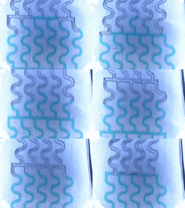
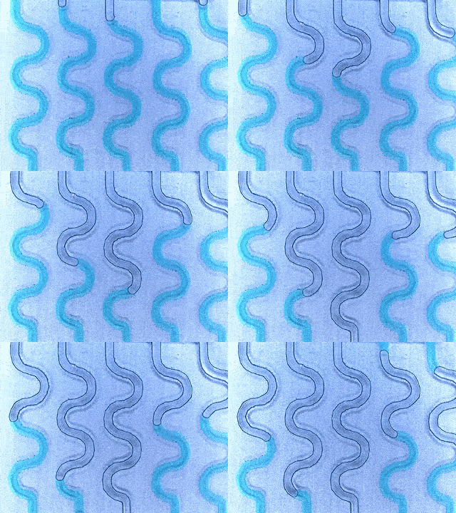
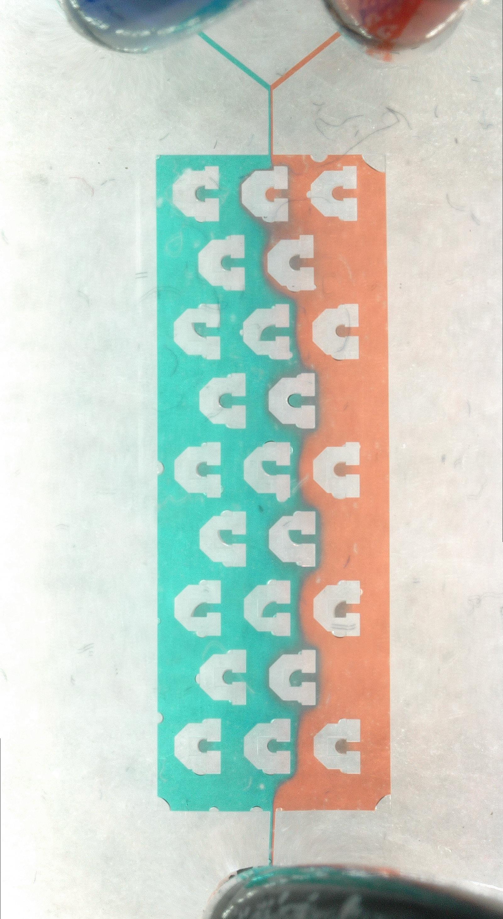
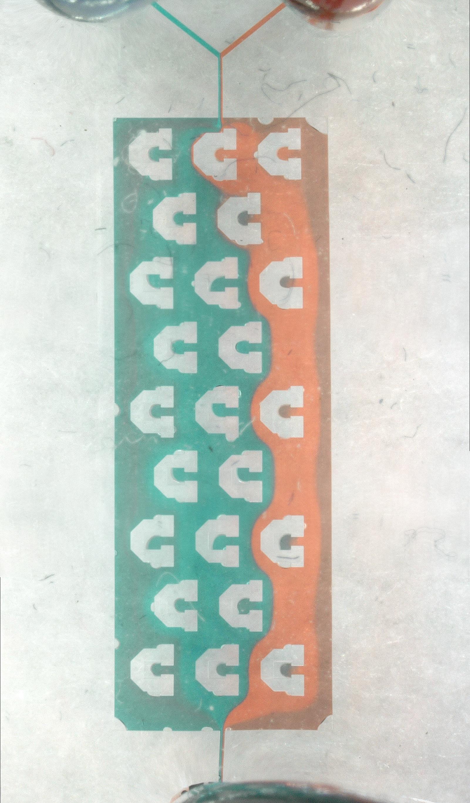
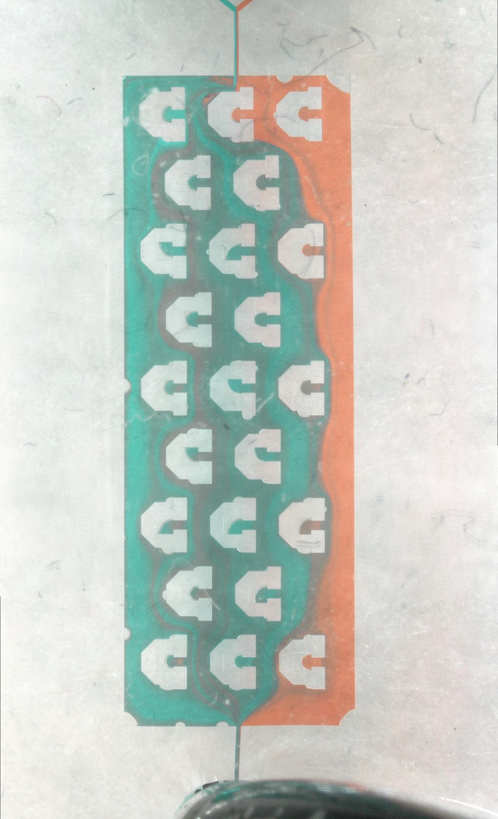
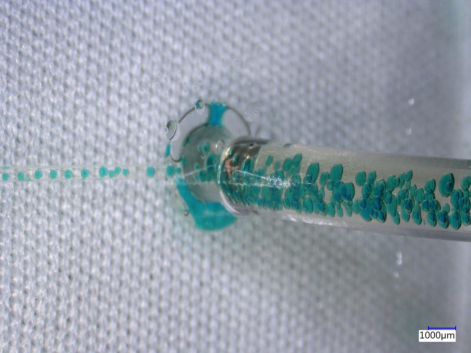
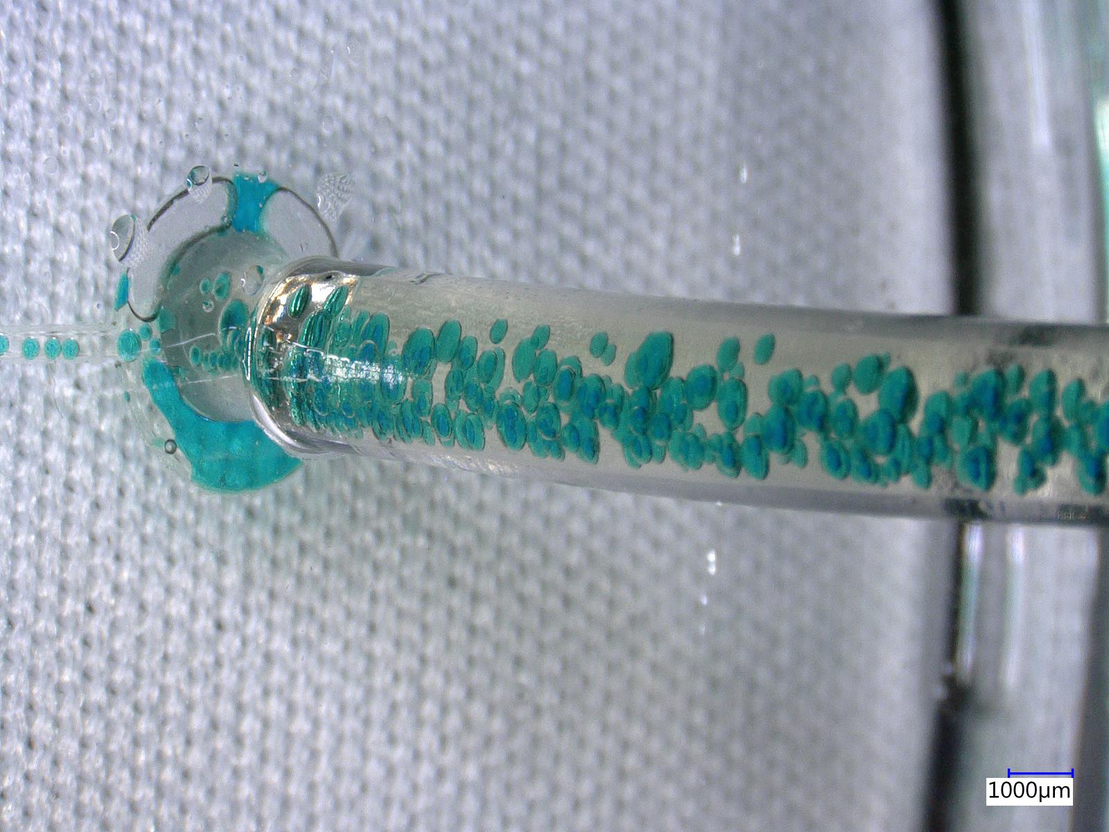
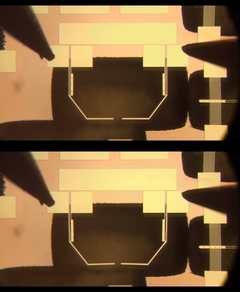
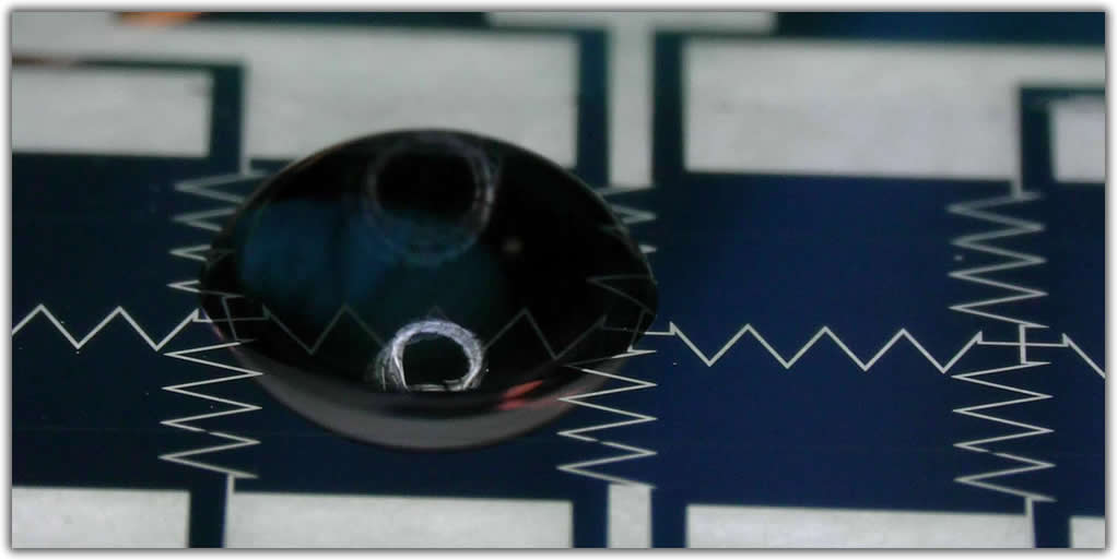 Microfluidics is a disciplinary field with applications in the design of systems dealing with small volumes of fluids, typically in the range of micro to nanoliters. In microscale devices, physical properties that are naturally intuitive in the macro-world often scale down in unexpected ways. The design team was tasked with designing microfluidic-related devices that could be used in high school and college level labs to introduce and teach students about the nuances in micro engineering. The microfluidic devices are often called lab-on-a-chip (LOC), so called for their ability to integrate laboratory-sized functions into chip-sized devices. They are made from a nontoxic biocompatible silicone polymer material called polydimethylsiloxane (PDMS). These devices needed to be interactive, low cost, and clearly demonstrate the unique scaling effects of a particular microfluidic phenomenon and its applications.
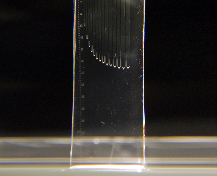
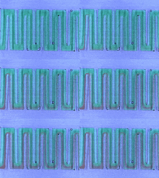
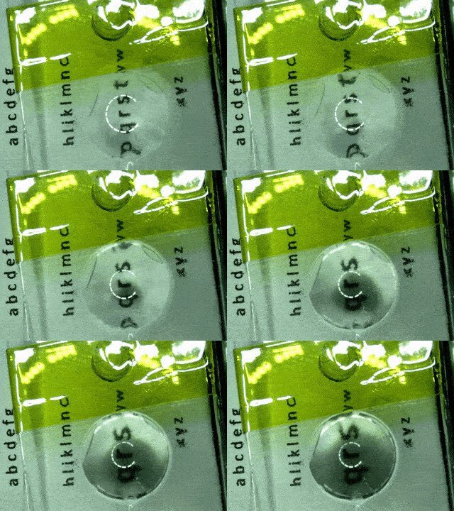
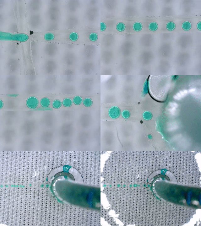
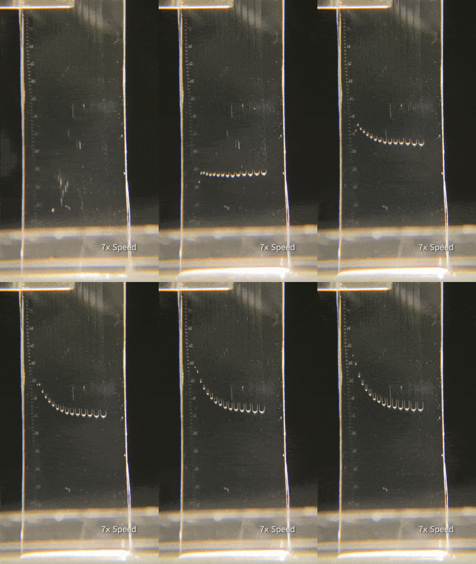
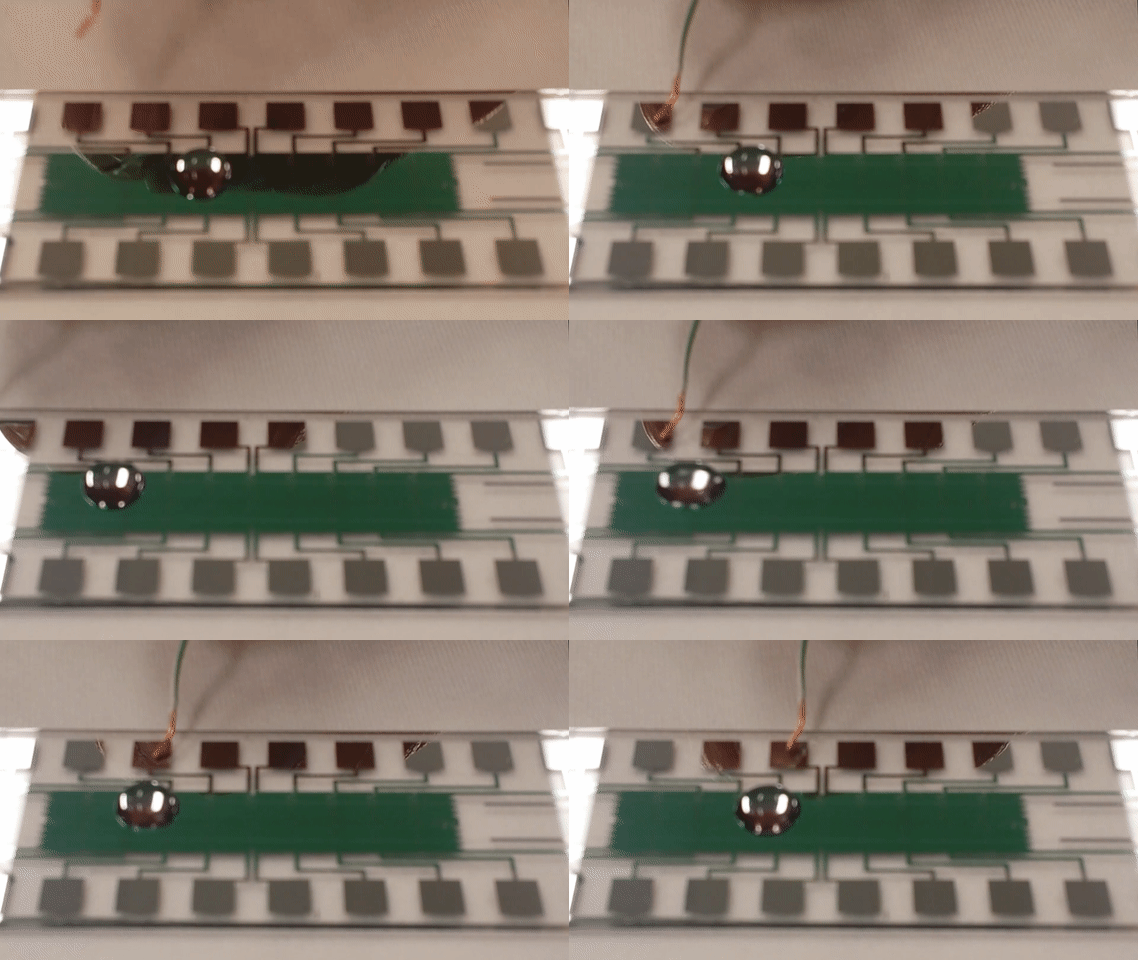
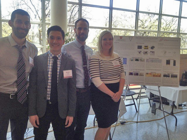 Design Team. Left-right:Samuel Feinman, Bryan Tran, Christopher Stolinski, Erika HancockThe microfluidics design team was comprised of four senior mechanical engineering students. Brought together by their mutual interest in micro and nanoscale engineering, the team was assembled to embark on a yearlong capstone project to research and develop microfluidic devices and teaching material. Each member designed and fabricated two microfluidic devices that exhibited unique phenomena. Erika provided devices that displayed laminar mixing and fluidic optics. Christopher researched devices that produced micro-sized droplets and developed a way to achieve laminar mixing with manually activated pumps. Bryan developed devices that demonstrated capillary action in microchannels and electrowetting on dielectrics. Samuel produced a method to affect laminar mixing by manually controlling the flow in microchannels using mechanical pin valves.
Images and Videos of Microfluidics Scaling Demonstration Devices
Detailed white paper report
Poster Presentation
MEMS Scaling Engineering Lesson Plans and Presentations
Please contact Dr. Ian Harvey if you are interested in buying your own Class On A Chip.
Click HERE to watch videos about how things are made at the Micro/Nanoscale
Images and Videos of MEMS Scaling Demonstration Devices
Utah Nanofab’s In-House MEMS Architecture
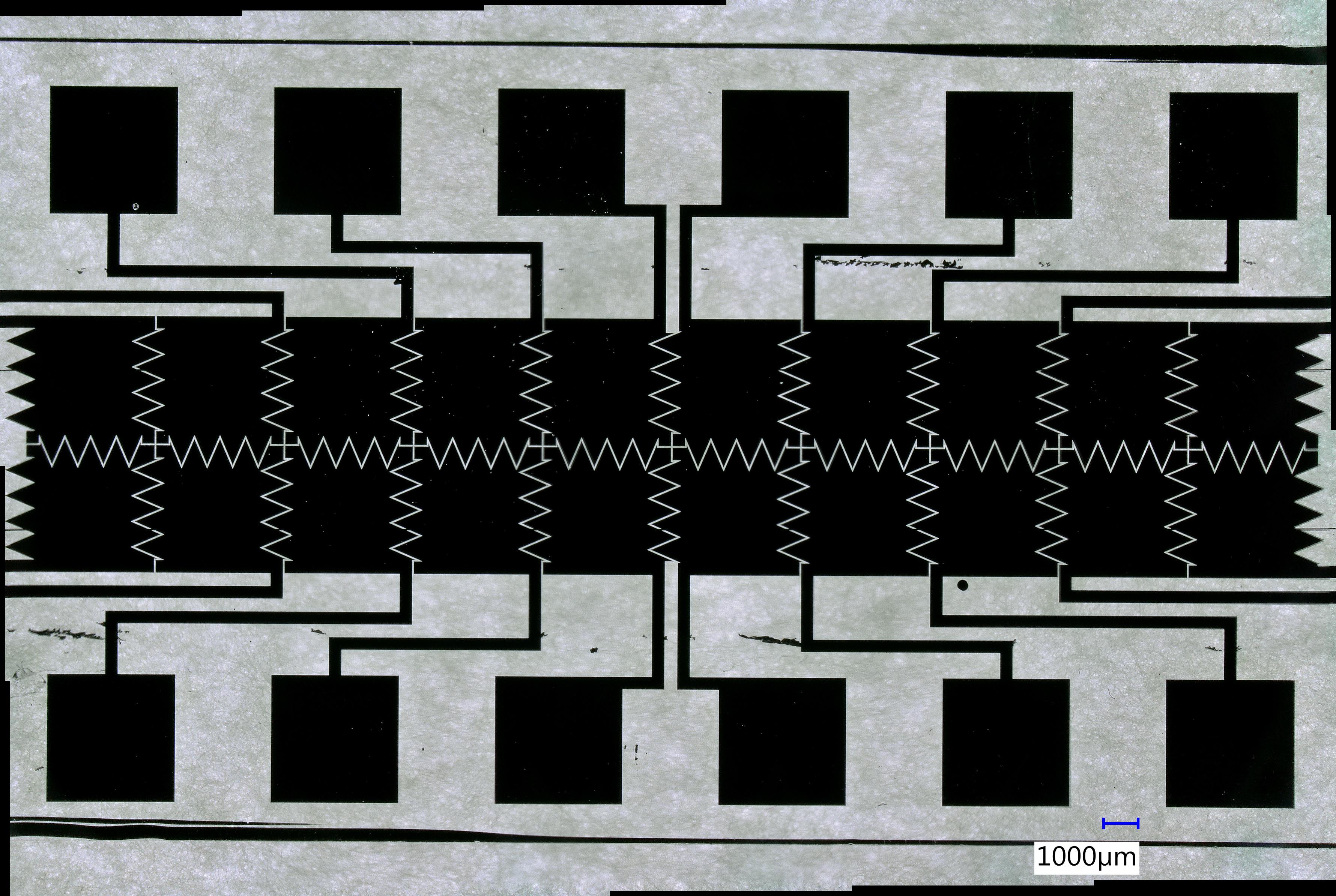
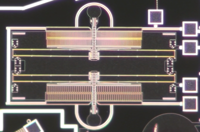
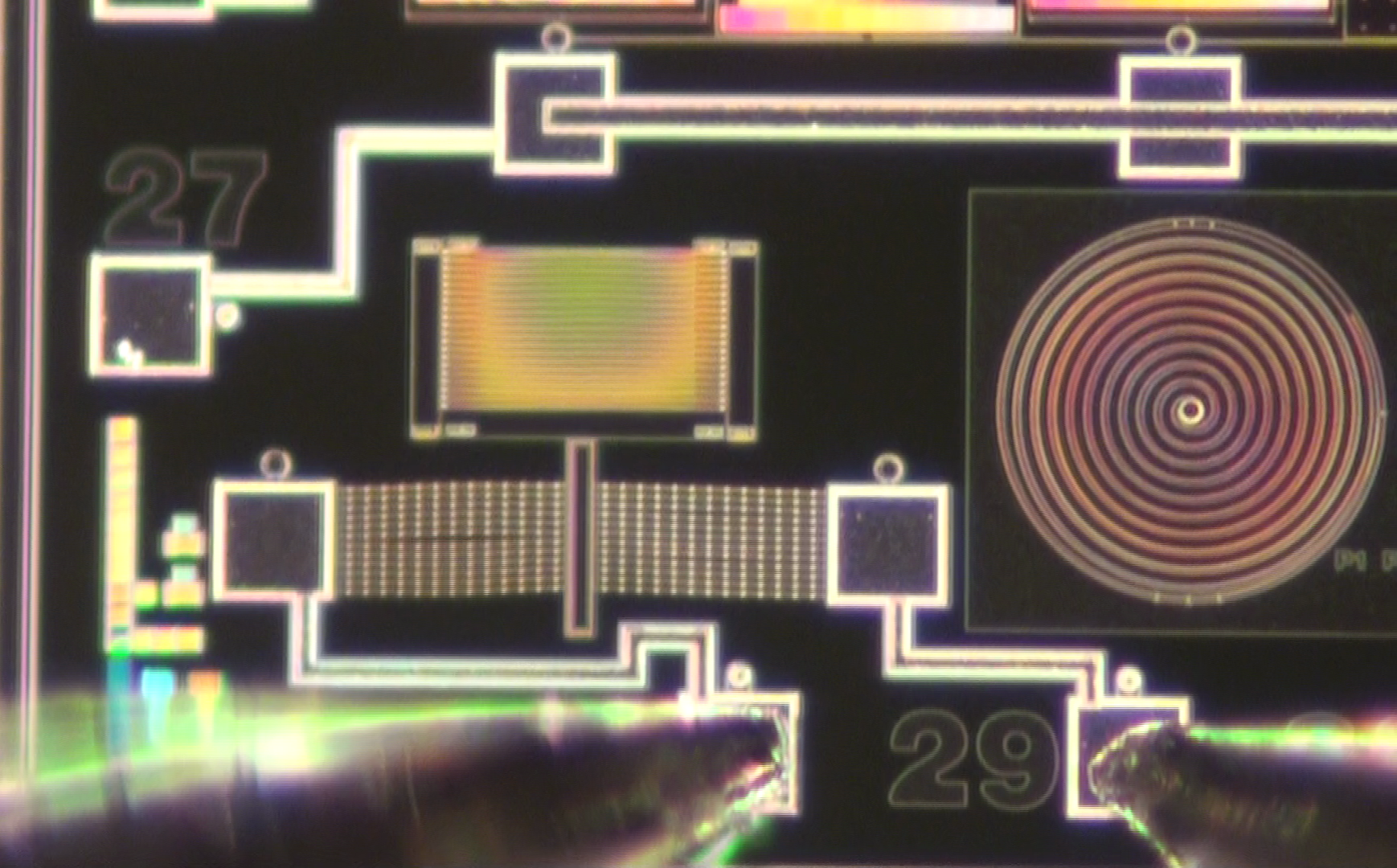
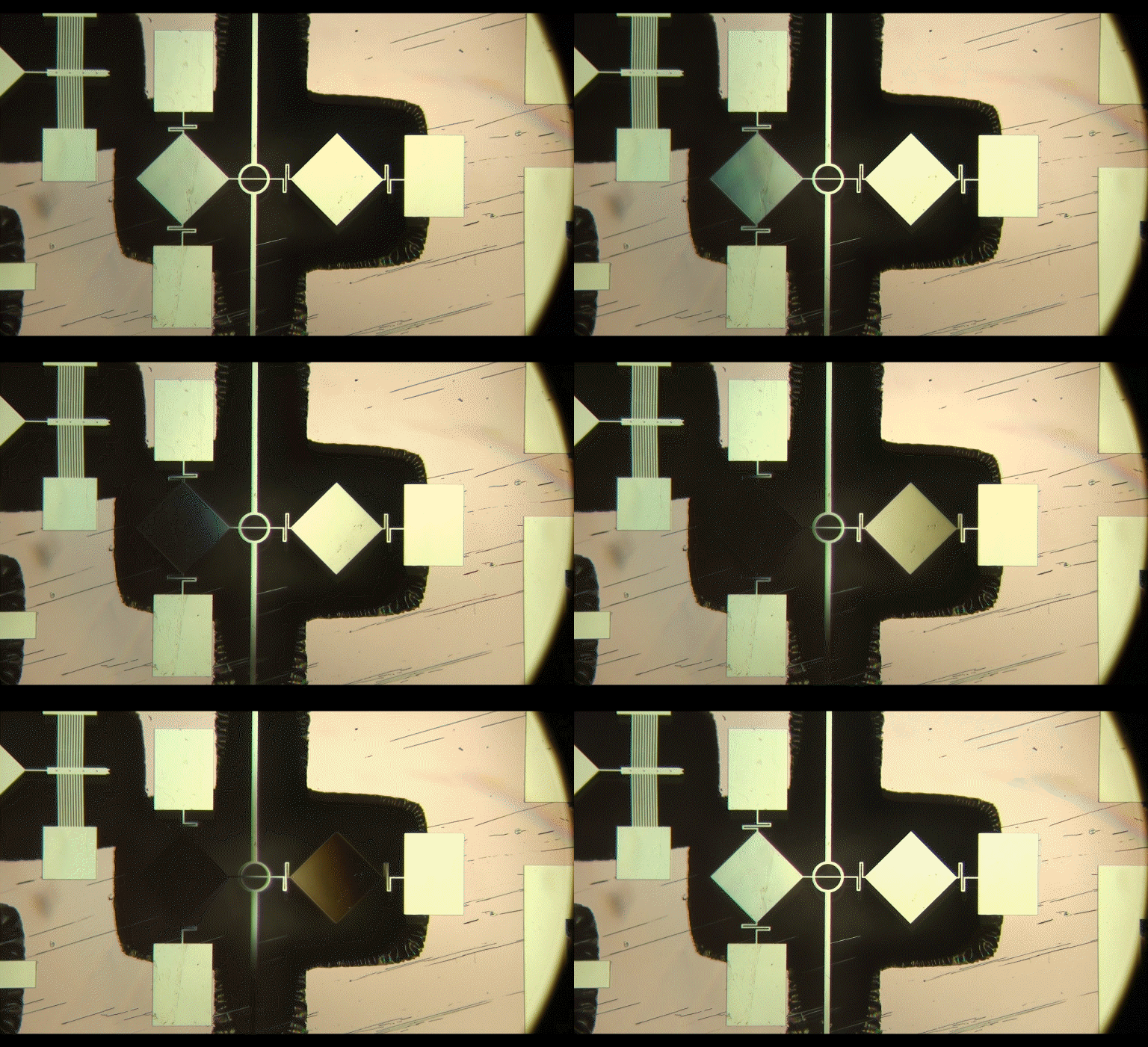
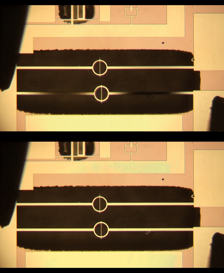
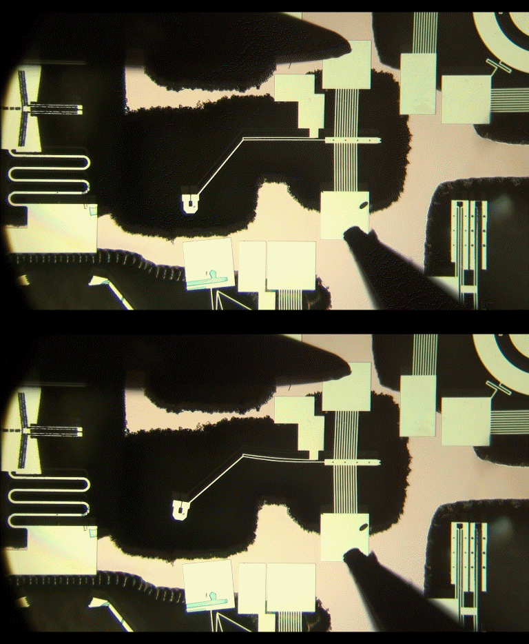
Initiated as an alternative to the Sandia SUMMiT VTM process, the University of Utah Nanofab has researched and developed a MEMS architecture that can be completed in our own facilities. The process consists of MEMS devices built from a single layer of silicon, thus they are not nearly as capable as the Sandia five-layer process in terms of versatility and complexity, but they have the advantage of being fabricated within a semester’s time and at a fraction of the cost. Additionally, the in-house process is able to produce devices which can still effectively convey and teach the same scaling principles as those listed above. Students will be able to learn about MEMS and fabrication techniques, then design their own MEMS devices, and have a chip back in time to test before completing a course.
Overview of fabrication process
Please contact Dr. Ian Harvey if you are interested in buying your own Class On A Chip.
Click Here to See more Videos about MEMS
MEMS University Alliance website where additional material will be posted.
* Note: this list is continually being updated as the project progresses. We also take suggestions for additional topics. Please provide feedback on how we can improve, and give us your modifications on how you made the content better.
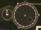
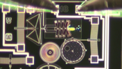
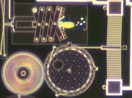
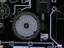
Utah engineering students have a unique opportunity to work in both the design and the manufacturing spaces for MEMS (Micro Electro Mechanical Systems), sometimes beginning early on in their academic program. The Utah nanofab hosts about ten courses that use the available thin film deposition and patterning tools, along with the sophisticated analytical tools of the Surface Analysis and nano Imaging lab.
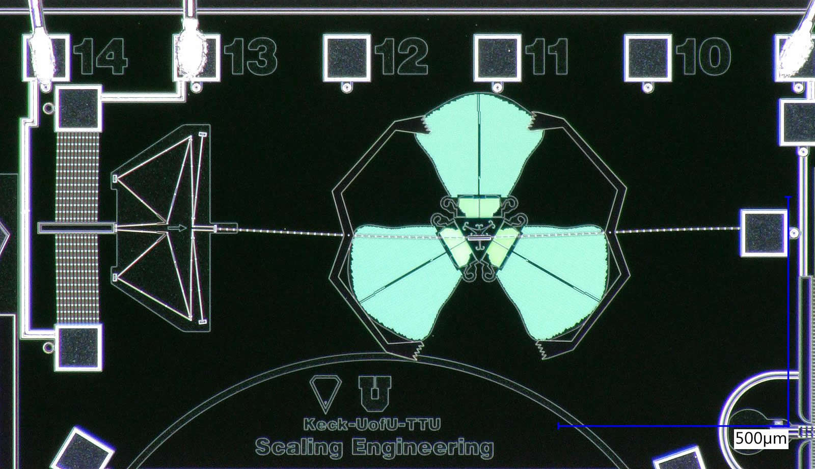
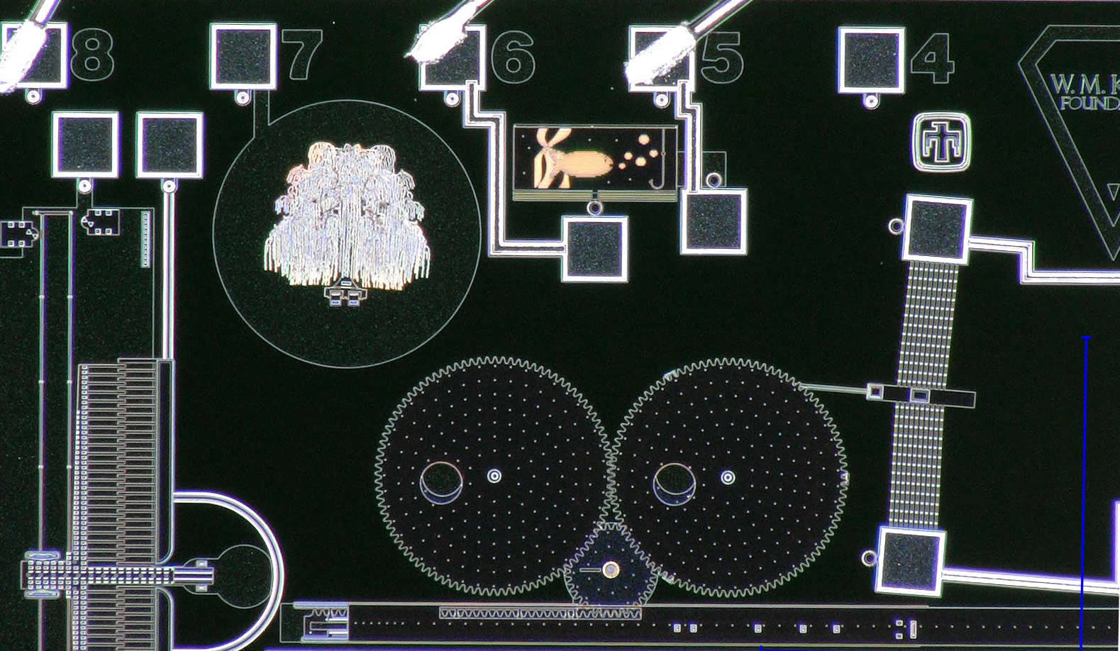
 From the design side, our students find that pure MEMS design opens a world of creative engineering without having to deal with difficult and expensive manufacturing issues. In one of our courses, Heterogeneous Microsystems Technologies, highly complex chips are fabricated for our students at no charge due to our participation in the Sandia National Labs University Alliance design competition, using the most advanced, billion-dollar surface micromachining process in the world. View the Video
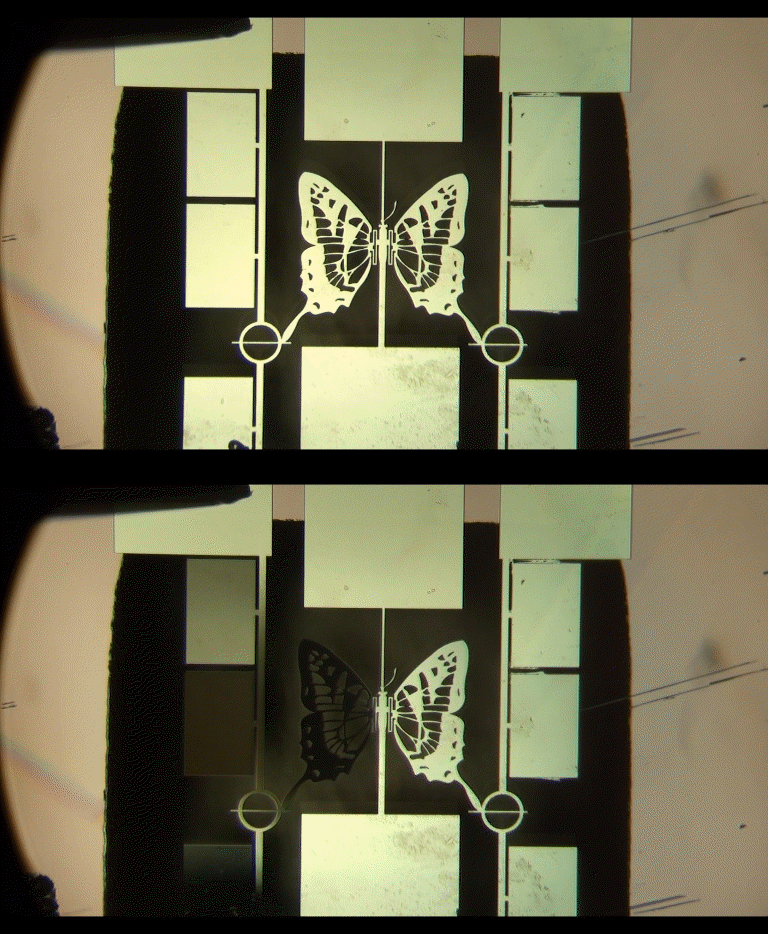
An example of this is Kinetic Micro SculptureTM, spontaneous movement of micro-meter scale art forms when imaged in a scanning electron microscope. This was envisioned by Mechanical Engineering faculty member Ian Harvey and prototyped and patented with a group of undergraduates; then brought to fruition by Harvey, Sandia Superuser Brian Baker, Prof. Paul Stout (Art), and undergraduate students Alex Hogan, Kurtis Ford, Kathryn Ecsedy, and Andrew Paulsen in a classroom setting. With the classroom success came extended funding through a grant from the University of Utah Center for Interdisciplinary Arts and Technology, and fabrication services were again provided through the generous support of Sandia National Laboratories, MEMS Technologies Department and the University Alliance competition.
Freshman student Kathryn Ecsedy (MechE) presented work from the 2009 Kinetic Micro Sculpture team in a Berlin conference on Knowledge, Technology and Society.
View the video Kathryn showed in Berlin.
Third-year participant Alex Hogan (Junior, ECE) and second-year participant Kurtis Ford (senior, MechE) were awarded summer internships at Sandia National Labs, acknowledging their passionate efforts during multiple years of intense competition.
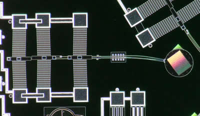
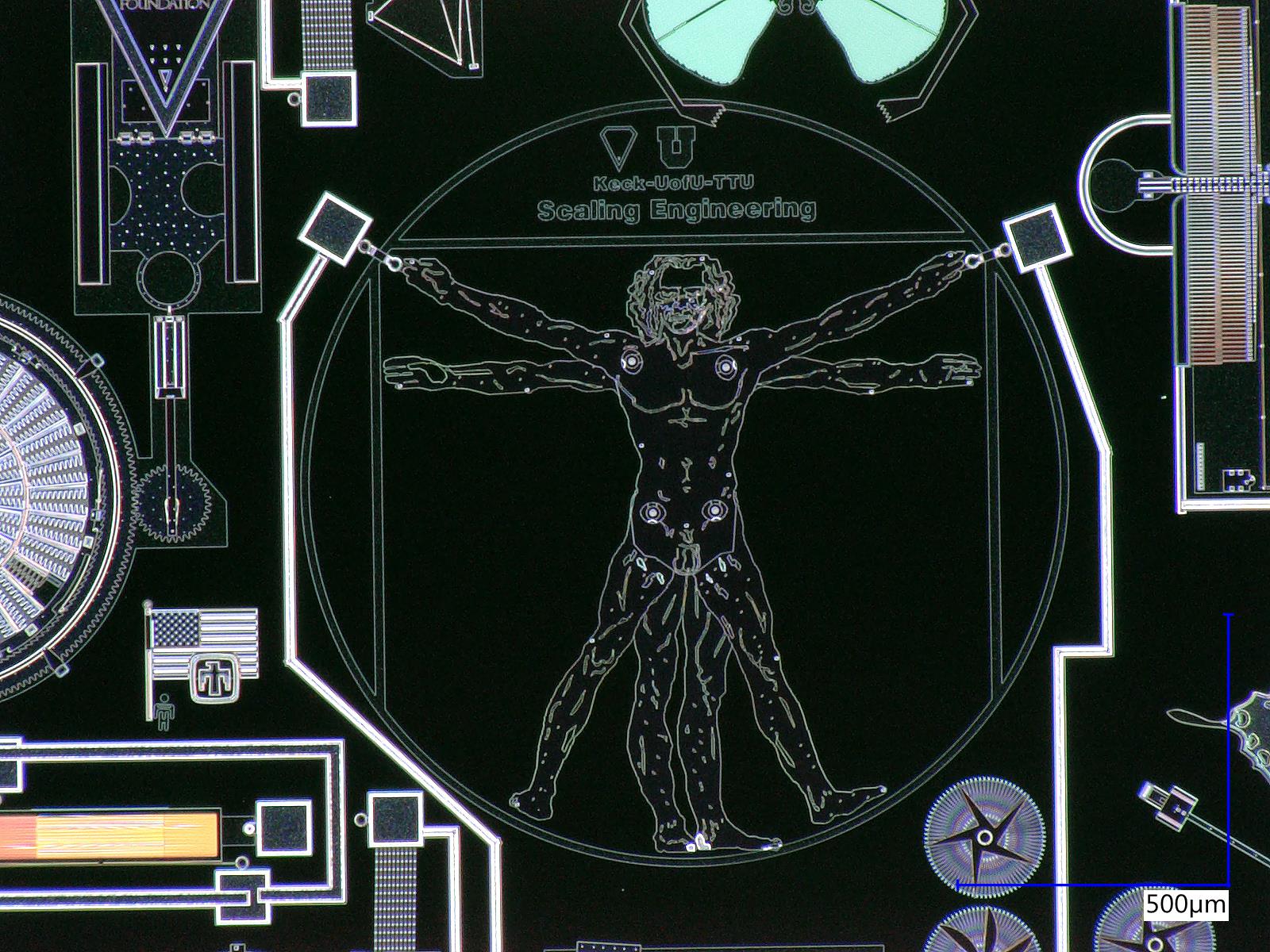
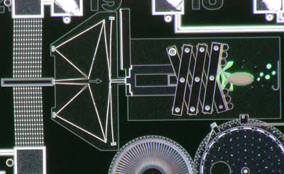
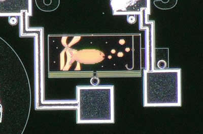
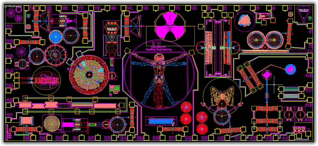
On th e 2010 team, winners of the Sandia competition education division, students Kurtis, Alex, Austin Welborn (M.S./B.S. student, MechE), Ted Kempe (Senior, MechE), Keng-Min Lin (M.S. student, MechE), Charles Fisher (MechE), Brian Baker, and advisor Ian Harvey submitted designs that will occupy space on two silicon chips, each approximately 2mm x 6mm. They presented their work at an invited seminar and awards program on May 18, 2010 at Sandia National Laboratory, in Albuquerque, NM. Their creative efforts have been highlighted in Popular Science.
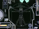
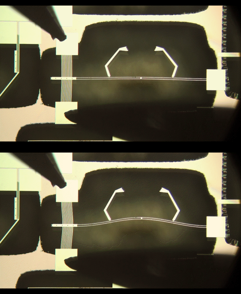
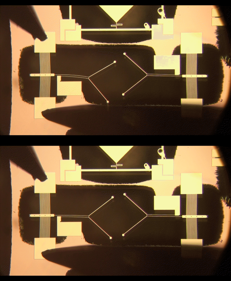
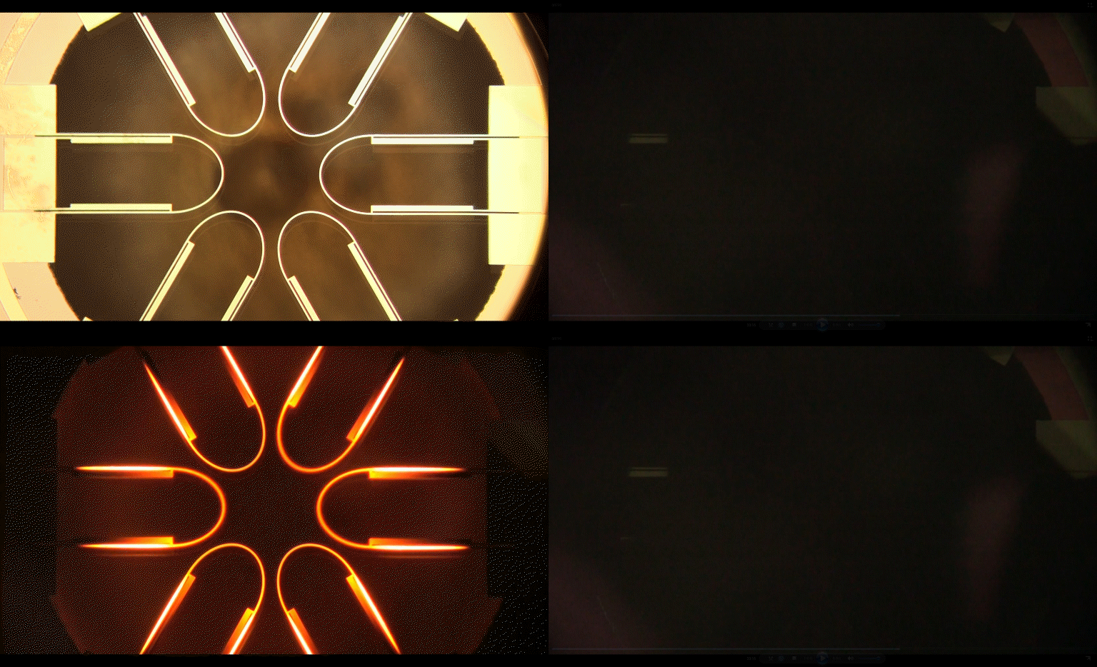
Designs included Austin’s microscale rendering of DaVinci’s Vetruvian man, mechanical lion, and mechanical wings; Kurtis’ unique microscale effort to demonstrate compliance in MEMS elastic materials by flipping a tiny loop of polycrystalline silicon inside-out, like a rubber band (powered by Charles Fisher’s gear reduction system); Alex’, Kurtis’ and Ian’s biomimetic adaptive lens actuator; Ted Kempe’s microscale tribute to the Hoberman arch in compliant beams; Keng-Min Lin’s microscale levitation micro-railway; Austin & Ian’s microscale self-erecting monolith tribute to “2010 – A Space Odyssey”, and Brian Baker’s microscale hair salon that grips a single hair, cuts it, dries it, teases it, and tips a mirror so the salon customer can see the micro-fashionable result.
All these devices play into an overall strategy to demonstrate and teach specific physical principles and consequences of dimensional downscaling to the micrometer level. These are all intended for use as a set of combined outreach demonstrators on-chip, for tour groups and interactions with grade K-12 students to stimulate interest in the visual ‘coolness’ of both constructing and seeing machines at the micrometer scale and below to nanotechnology.
See more cool videos about Micro Engineering:
Snowbird Resort Magazine Ad
The College of Engineering will be highlighting the work of Assistant Professor Mike Scarpulla in Materials Science & Engineering in a recruiting advertisement to be featured in a Snowbird resort magazine. You can view the advertisement here.

