Services Include:
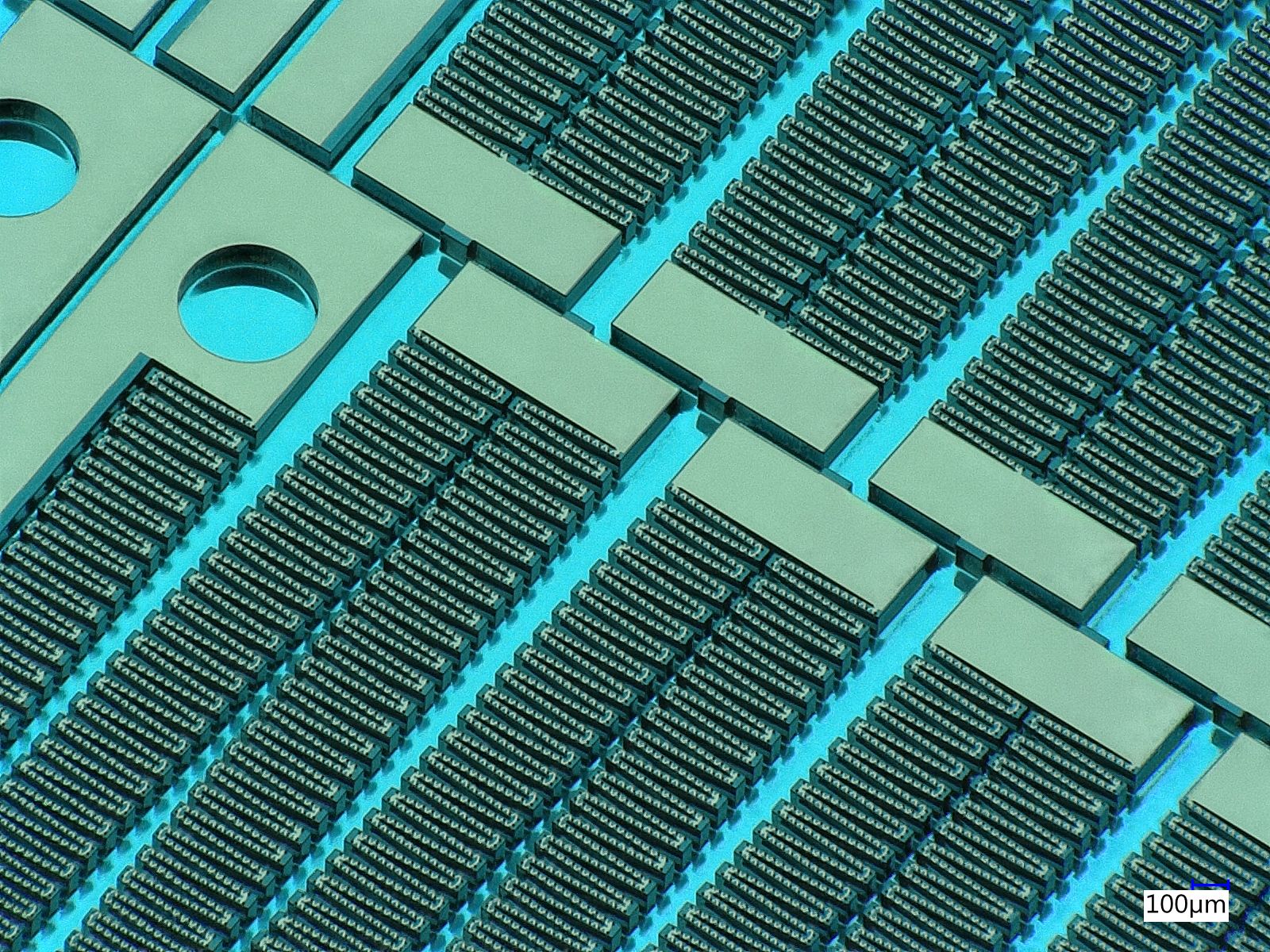
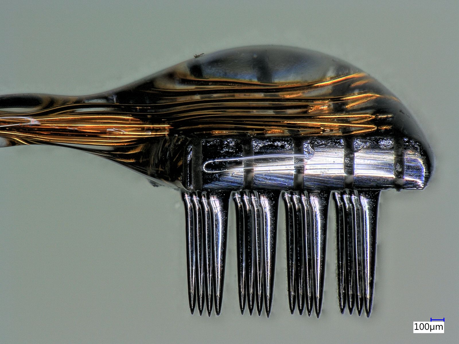
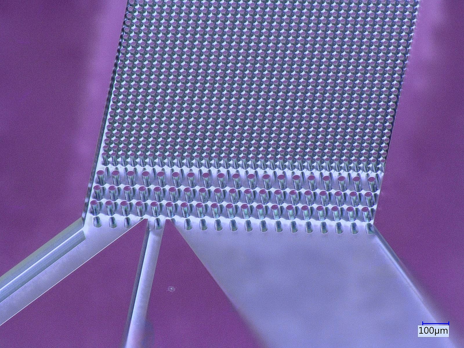
*Soft Lithography (SU8 master mold & PDMS molding and bonding to glass or silicon)
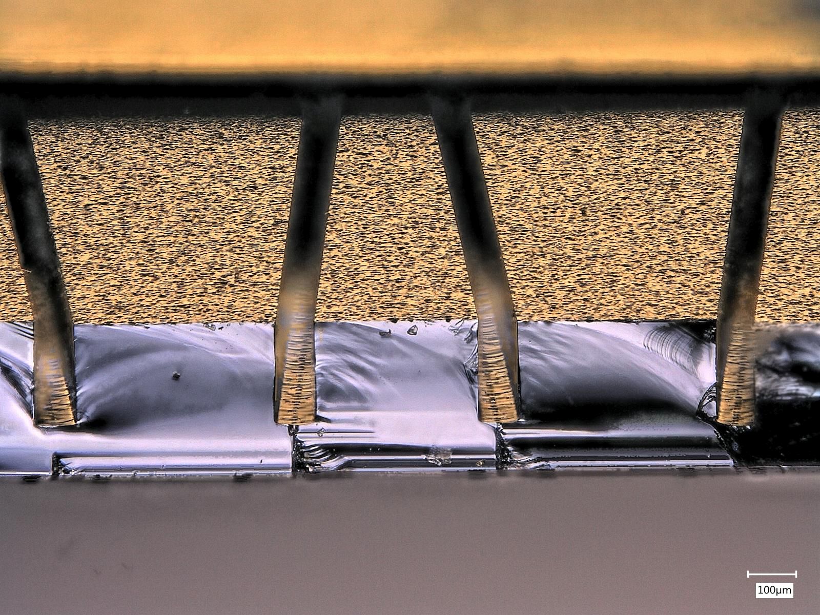
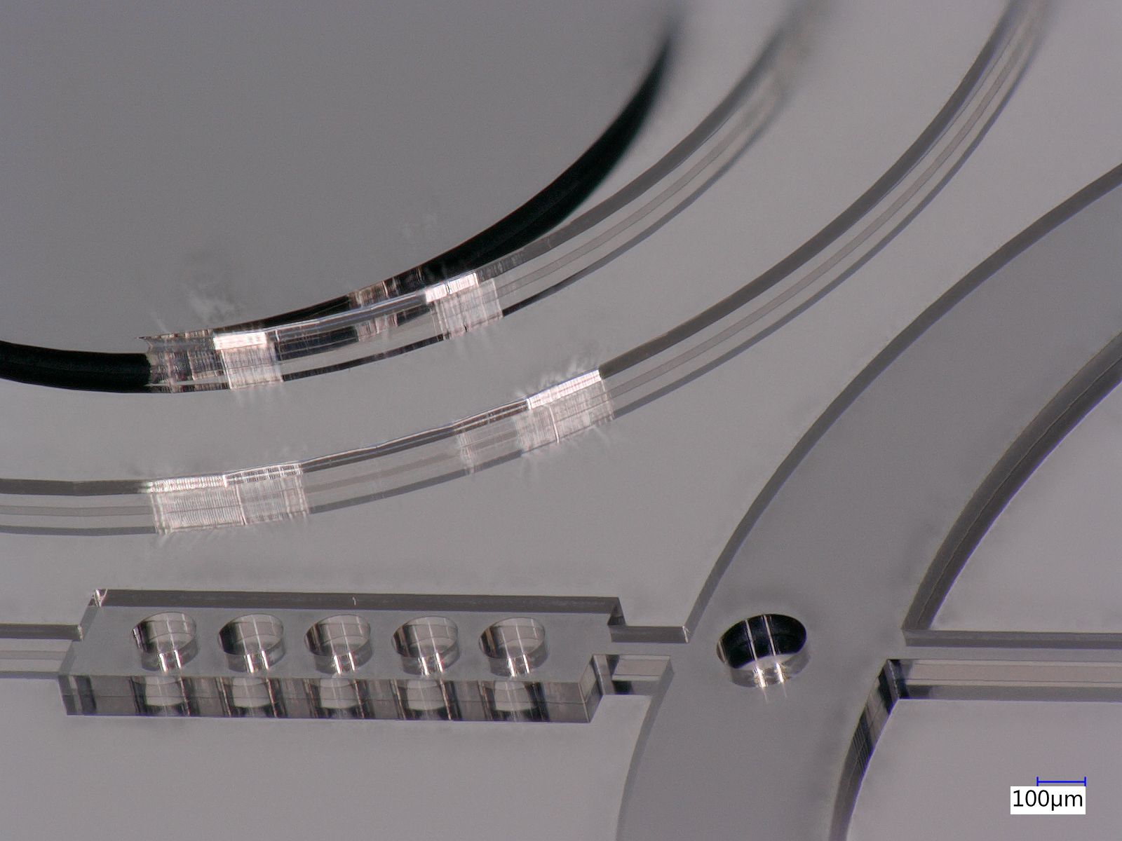
*Silicon DRIE microchannel etching, including through-wafer aligned channels
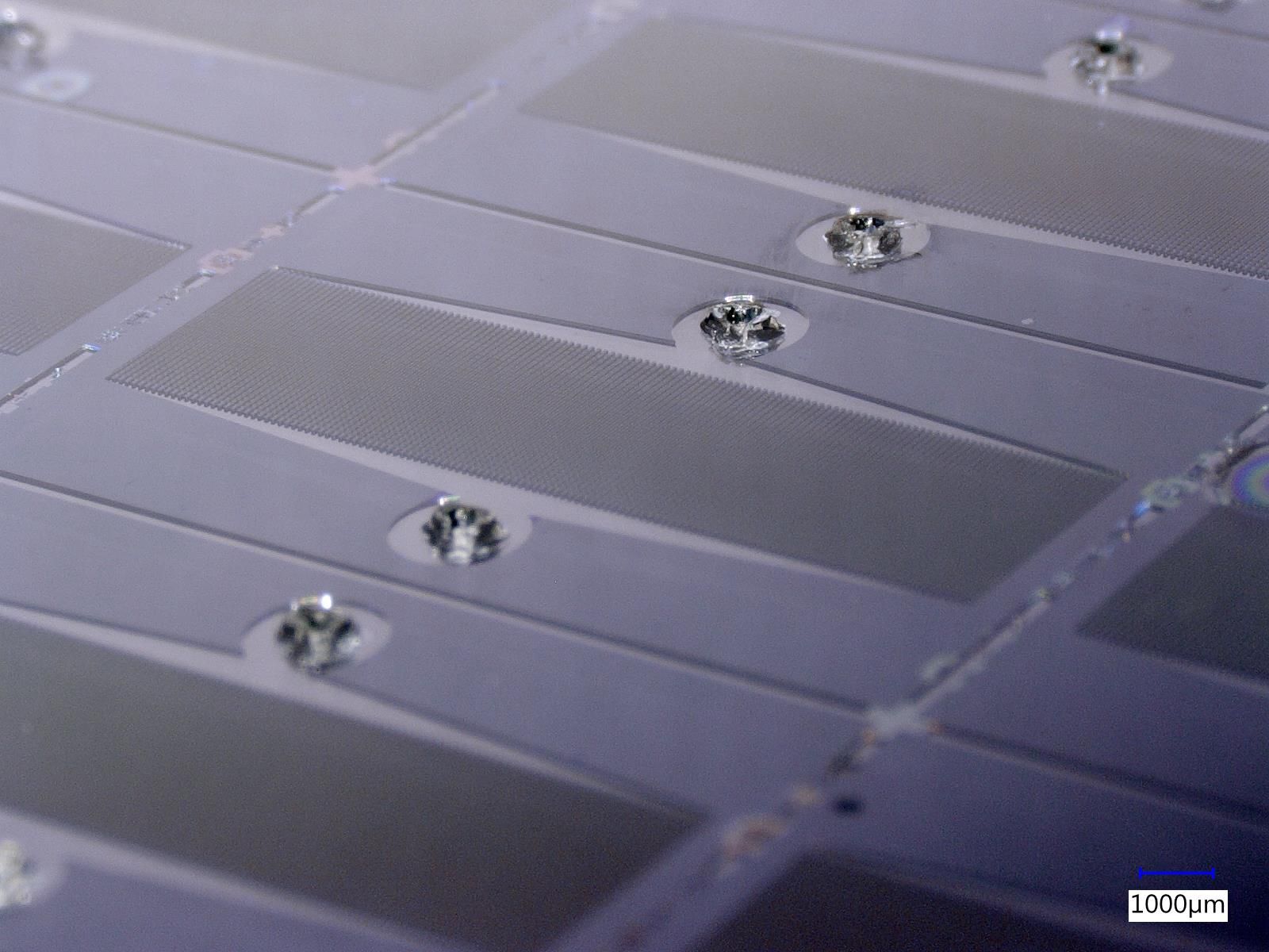
*Anodic bonding of silicon microchannels to borosilicate glass
*Laser cutting of vias in borosilicate glass
Contact Nanofab Cleanroom staff with device design, details, and specifications https://www.nanofab.utah.edu/lab-staff/#process (Brian Baker)
Staff will work with you to determine the best fabrication process and then give you an estimate for total time and cost
Set up a Nanofab account (https://workauth.cores.utah.edu/#/offcampus)
After you approve/authorize the design, staff will manufacture and ship your devices/chips/wafers to you