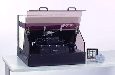
Tool Owner
Brian Baker (bbaker@eng.utah.edu)
Reservations Calendar

- S/N DWL646
- Accepts DXF/CIF/BMP file formats
- 3 um minimum feature size (Smaller features possible)
- 3″ x 3″, 4″ x 4″, 5″ x 5″ chromium masks and direct wafer write
- Light field or dark field selectable in system control software
SOFTWARE:
- L-Edit CAD Layout Software
- AutoCAD software
- Intellisuite and Cadence design and simulation software (CADE lab)
- DXF/GDSII/CIF file software conversion tools
PROCEDURE:
MASK MAKING STEPS
Consult with Nanofab staff regarding microfabrication process flow and mask design.
Design mask using AutoCad or LEdit
Mask size depends on wafer size, typically:
- 2” and 3” diameter wafers: 4” mask
- 4” diameter wafers: 5” mask
Mask polarity depends on deposition and etch processing:
- Liftoff using positive photoresist – Dark field (Transparent where film should remain after liftoff)
- Etching using positive photoresist – Light field (Opaque where film should remain after etch)
GENERAL DESIGN RULES:
• Keep in mind that defined areas will be exposed.
• Do not use special characters (spaces, punctuation marks, umlauts ..) in the design name.
• The design coordinate origin must be the center of the design.
• If possible, create the whole design in only one layer. If several layers are used, they will be merged using an OR function.
• All polylines must be closed. Keep in mind that interiors of polyline structures will be filled out completely, covering any structures within.
• Do not cross polylines, or create doubled vertices (vertices with no distance between them). This will create data errors.
• Do not use single lines without width.
• Limits:
- maximum design size: 100mm x 100mm
- 1,000,000 vertices/polygon
- maximum definition or reference depth: 16
- maximum number of definitions or references: 100,000
DXF SPECIFIC DESIGN RULES:
• Use a 100% AutoCAD compatible editor.
• The design has to be created in metrical units.
• As far as possible, only use the structure types “polyline”, “circle”, and “text”.
• Only one text font is provided. This will replace any other font used in the design creation. The only supported text attributes are “rotated”, “mirrored”, and “scaled”.
• Try to use as few layers as possible. All layers will be merged via an OR operation.
• Do not use special characters in the layer names.
• Polylines with width must not change their width (tapered lines).
• When inserting blocks, the same scaling has to be used for x and y.
• External blocks are not supported.
BMP SPECIFIC DESIGN RULES:
• Maximum image file size is 4 GB.
• For grayscale exposures, use 8-bit format. The 256 gray values will be interpolated down to 100 gray values.
• Create the design in a 90° counter-clockwise rotated version, as the design will be rotated 90° clockwise during data processing.
CIF SPECIFIC DESIGN RULES:
• Use only one layer. If several layers exist in a design file, only the layer with the most references will be written.
• Maximum definition or reference depth is 50.
• The subroutine with the highest number definition will be taken as main routine.
Download Files
Files
SOP:
Spec Sheet:
Member Files
Characterization:
Grayscale tests -1 Grayscale tests -2
Staff Files
Manuals:
uPG101_PI1_Preinstallation_Guide.pdf
uPG101_UG1_Addendum_Option Multiple Exposure.pdf
uPG101_UG1_User_Manual_Rev5.pdf
SOP:
Special Instruction:
Special Instructions: